How a CPU Works
Roger Ngo, <rogerngo90@gmail.com>, http://rogerngo.com
Interpreting Code
The CPU is a very useless piece of electronics when compared to a machine that has been constructed and wired to do a specific operation -- like an oven. The CPU cannot really do anything useful without software to tell it what to do. Software is a a composition of instructions written for the CPU to drive the CPU to perform operations that are deemed useful. Computer hardware and software must coexist with one another for any practical use.
For a complete computer system, instructions from some source, usually by ROM or secondary storage is loaded into memory. The CPU is wired to look at a specific location in memory (address) and begins executing these instructions. Each instruction will tell the CPU to perform some sort of basic operation. Instructions when executed, modify the CPU state one after another. As the state of the CPU changes, each instruction is no longer arcane and begins to tell a story.
CPU instructions are stored as binary digits. Zeros and ones. The instructions are grouped into a number of bits. In this grouping of bits, a number are allocated to be defined as the "opcode". The opcode is essentially the smallest addressable unit of instruction that will guide the CPU to perform some sort of logic with a specific set of operands. Think of opcodes as a key to a specific set of doors. The objects that flow through the doors, are the rest of the bits within the group.
The software engineer, or programmer does not naturally write these CPU instructions as binary. The engineer will actually compose the program in what we call a programming language. This programming language is essentially the set of statements that the engineer wants the CPU to interpret as instructions. These statements are input into an assembler which then translates the statements into assembly language. Assembly language is then a 1:1 representation in mnemonic, of the binary instructions that will then be fed into the CPU.
Lets take a look at how programs are written in a programming language, are turned into binary bits, and in turn are interpreted by the CPU.
A program will have a set of statements. For example, the statement in a C-like language stores the number 2 into variable x.
int x = 2;
x = x +1;
In 6502 assembly, this statement will be translated into:
lda #$2
sta $8000
lda $8000
inc a
sta $8000
The above assembler will load the value 2 into memory location $8000, which is essentially the location of our x variable. Then the value is incremented and stored back into the same memory location.
Therefore, the flow of translation of program statements into CPU instructions can be modeled:

Then this binary data will be loaded into memory with the program counter (PC) set to a specific location by the CPU and will begin execution.
Physical Architecture
A CPU can be physically made of individual circuits that can be switched on or off. A combination of these circuits will then create logic that will cause electricity to flow in and bring the CPU into some sort of state that can be interpreted as a result. Having large physical circuits to construct a CPU is not scalable as earlier computers took up the entire space of large rooms -- more powerful CPUs would need space that would be impossible to manage. Therefore, transistors are what modern CPUs are now composed of.
A transistor can be thought of as a very tiny switch that will simply turn a circuit on, or off. Therefore, each transistor will represent either a 0 (off) or 1 (on). The combination of the transistors will create logic. Logic is then chained together to make data paths that will allow the CPU to physically take itself into various states.
It is the program that the software engineer write that will utilize the available logic in the CPU to make things happen. However, logic just doesn't happen. Logic must be paced and is driven by a clock. 1 MHz for example, is a clock frequency a CPU can run at. One million cycles per second.
Generally, a CPU will consist of the following components:
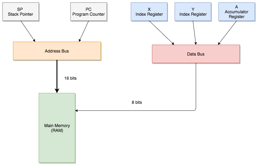
Control, data and address lines are used to communicate to external devices through a system of lines (wires) called "buses". In the 6502, the data and control buses are 8 lines -- one for each bit, while the address lines consist of 16 lines -- 16 bits. This gives the 6502 16-bits of addressable memory, which is 64 KB (2^16 bytes).
It is important to note that it is the control and data lines in the bus that defines the "bit-ness" of a CPU.
General purpose registers are used to store intermediate results within the CPU operations. The 6502 consists of 3 general purpose registers:
The registers above are all 8 bit registers and thus store one byte of data.
Special purpose registers belonging to the 6502 are:
The communication between the general purpose registers are made through the 8 bit data bus, while the stack pointer and program counter are actually 16 bit registers that communicate with memory through the 16 bit address bus. The following block diagram shows how each register makes a link between the various buses to form a communication system:

Fetch-Execute Cycle
The program counter (PC) register stores the current 16-bit address of the instruction to be executed next in memory. The PC can be increment sequentially, or modified through the use of branch and jump instructions. There are usually two modes for the latter -- absolute offsets and relative offsets. As you might see later down the line, JMP type instructions modify the PC register in an absolute fashion. That is, the address is directly assigned to the PC register. In the relative offset approach, branching instructions such as BCC, BNE, etc will actually modify the PC by subtracting or adding a value between -128 and 127.
A program usually consists of the two important pieces of information:
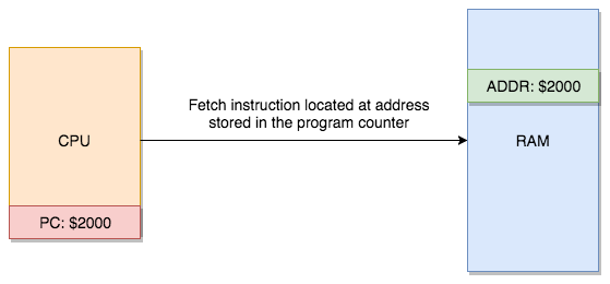
The program is loaded into RAM. The CPU must look into memory and fetch in the instructions and data and act upon them according to what the instructions are.

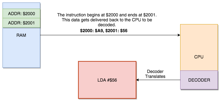
The RAM, in response will deliver back the instruction based on the address to the instruction register. As each instruction is fetched from memory, it is placed into the instruction register (IR) and decoded.

The control unit performs the decode of the instructions and generates all the data and signals needed to manipulate the state of the CPU. Note that I define the state of the CPU through augmentation of the registers.
A typical instruction for the 6502 will consist of 1-3 bytes. It is composed:
The instruction always begins with an opcode. It tells the CPU what operation will be carried out. The opcodes are typically 1 byte. The next part of the instruction is the operand. Operands can be any of the following: data, memory address, value, etc. The CPU will just operate on this value based on the opcode.
How does the CPU know which instruction to fetch first? The CPU will know where to look for the first instruction in memory through the use of a memory map. The memory map is an abstracted map of how RAM is laid out. When the program is first loaded into RAM, there is a region in which the program must be loaded into. For the 6502, the directive in many assemblers is ORG, or origin address. By defining the address with the ORG directive, the CPU will know where to begin in memory, execution of the program.
An example would be something like this:
.ORG $2000
LDA #$56
This will tell the CPU to start processing the instructions at address $2000.
Let's reiterate on the fact that the PC actually points to the next instruction to be executed. Basically, the opcode is fed into the control unit. The PC is incremented. Based on the opcode, the CPU will decide if more bytes will need to be fetched. If so, then the CPU will fetch the operands and increment the PC on the fly. The CPU does this so that the PC always points to the next instruction. Knowing this very important fact is crucial in keeping track of how the CPU is executing through program data.
ALU
The arithmetic and logical instructions of the CPU are executed in the ALU. The ALU is essentially just a construct of logic gates that allow the CPU to perform the following operations:
Through various combinations of instructions that employ the ALU, the CPU can get a lot done with just those operations. The 6502's ALU performs an operation and will usually store the result into the accumulator (A) register. At the same time, various ALU operations will then modify the status (P) register to signal to the programmer what meta information the ALU operation resulted in... whether the resulting value is negative, zero, etc.
Source: Microprocessor Technology. J.S. Anderson
Previous: NES CPU Specifications
Next: 6502/2A03 Architecture: